Adders
Addition is one of the most fundamental operations in computers. Integer arithmetic, address calculation, and even multiplication/division ultimately rely on adders. In CPU datapaths, adders are core components inside the ALU.
Half adder
Section titled “Half adder”A half adder adds two 1-bit numbers without a carry-in.
- Sum:
- Carry:
Truth table:
| A | B | S | C |
|---|---|---|---|
| 0 | 0 | 0 | 0 |
| 0 | 1 | 1 | 0 |
| 1 | 0 | 1 | 0 |
| 1 | 1 | 0 | 1 |
Table 2.5: Half-adder truth table.
Symbol:

Figure 2.4: Half-adder symbol.
A half adder cannot directly build multi-bit addition because it lacks a carry-in input, so we need a full adder.
Full adder
Section titled “Full adder”A full adder adds A and B with a carry-in :
- Sum:
- Carry-out:
Symbols / construction idea:

Figure 2.5: Full-adder symbol.

Figure 2.6: Constructing a full adder from two half adders and an OR gate.
Ripple-carry adder
Section titled “Ripple-carry adder”Chaining full adders forms an -bit adder. The carry-out of each bit feeds the next bit’s carry-in. With at the least significant bit, this is a ripple-carry adder.

Figure 2.7: 4-bit ripple-carry adder.
Ripple-carry adders are simple and great for teaching, but carry propagation makes delay grow roughly linearly with bit width, so modern CPUs use faster adder designs.
Experiment: Hierarchical adder design
Section titled “Experiment: Hierarchical adder design”Objectives
Section titled “Objectives”- Build a 1-bit half adder using gates.
- Build a 1-bit full adder in a modular (hierarchical) way.
- Build a 4-bit ripple-carry adder from full adders and observe carry propagation.
Environment
Section titled “Environment”- Simulator: Logisim Evolution
Task 1: Gate-level 1-bit half adder
Section titled “Task 1: Gate-level 1-bit half adder”- Place input pins A and B.
- Place output pins S and C.
- Build with one XOR gate.
- Build with one AND gate.
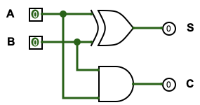
Figure 2.8: Gate-level 1-bit half-adder circuit.
Test (A,B) = 00, 01, 10, 11 and confirm (S,C) matches the truth table.
Task 2: 1-bit full adder (modular)
Section titled “Task 2: 1-bit full adder (modular)”- Rename the current circuit to HalfAdder.
Figure 2.9: Renaming a circuit in Logisim Evolution.
- Create a new circuit named FullAdder and set it as the main circuit.
- Place inputs A, B, and ; place outputs S and .
- Place two HalfAdder subcircuits.
- First HalfAdder: inputs A, B; outputs ,
- Second HalfAdder: inputs , ; outputs S,
- Use an OR gate to compute .
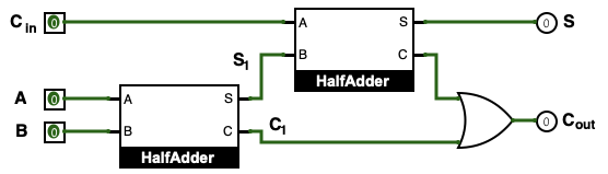
Figure 2.10: 1-bit full-adder circuit (hierarchical design using HalfAdder subcircuits).
Test all combinations (A,B,) from 000 to 111.
Task 3: 4-bit ripple-carry adder
Section titled “Task 3: 4-bit ripple-carry adder”- Create a new main circuit named RippleAdder4.
- Place 4-bit inputs A[3:0], B[3:0] and 1-bit input .
- Place 4-bit output S[3:0] and 1-bit output .
- Use splitters to break out bits A0…A3, B0…B3, S0…S3.
- Place four FullAdder blocks and chain their carries.
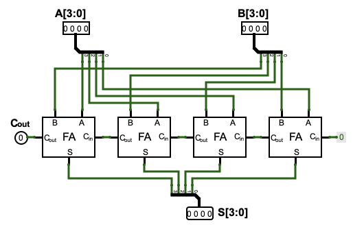
Figure 2.11: 4-bit ripple-carry adder circuit (FullAdder chained with carry propagation).
Functional checks (example test vectors):
- No carry chain: A=0010, B=0001 → S=0011,
- Multi-bit carry: A=1111, B=0001 → S=0000,
- Random vectors: verify against hand calculation
Observe carry propagation using an input that causes a continuous carry chain.
Results
Section titled “Results”- Half adder: circuit screenshot + truth table test screenshot.
- Full adder: circuit screenshot + test screenshots for 000…111.
- RippleAdder4: circuit screenshot + screenshots for at least 3 test cases + a screenshot showing carry propagation.
Extension
Section titled “Extension”- Package RippleAdder4 and extend it to an 8-bit adder; discuss delay impact of longer carry chains.
- How would you generate an overflow signal?