Multiplexers and Decoders
Multiplexers
Section titled “Multiplexers”A multiplexer (MUX) is a combinational circuit that selects one of multiple inputs to drive a single output, based on control (select) signals. Common types include 2-to-1, 4-to-1, and 8-to-1 multiplexers.
For a 2-to-1 MUX, the behavior is:
- If select signal S = 0, output Y = D0
- If select signal S = 1, output Y = D1
So the logic equation is:
See Figure 2.1.

Figure 2.1: 2-to-1 multiplexer symbol.
In general, if the number of select bits is n, the number of input lines is , e.g.:
| MUX type | Inputs | Select bits |
|---|---|---|
| 2-to-1 | 2 | 1 |
| 4-to-1 | 4 | 2 |
| 8-to-1 | 8 | 3 |
Table 2.1: Relationship between MUX input count and number of select bits.
Multiplexers are used everywhere in CPU datapaths, such as:
- selecting between data sources
- selecting register write-back values
- selecting ALU operands
- selecting program counter (PC) update paths
In CPU design, MUX selection is typically driven by control signals from the control unit, enabling a clean separation between control flow and data flow.
Decoders
Section titled “Decoders”A decoder does the “opposite” of a multiplexer: it converts a binary-encoded input into a one-hot output (exactly one output line is asserted). A typical decoder has n input lines and output lines.
For a 2-to-4 decoder:
- inputs: A1 A0 (2 bits)
- outputs: Y0 … Y3
- only one output is active at a time (here, active-high)
| A1 | A0 | Y0 | Y1 | Y2 | Y3 |
|---|---|---|---|---|---|
| 0 | 0 | 1 | 0 | 0 | 0 |
| 0 | 1 | 0 | 1 | 0 | 0 |
| 1 | 0 | 0 | 0 | 1 | 0 |
| 1 | 1 | 0 | 0 | 0 | 1 |
Table 2.2: 2-to-4 decoder input/output mapping (active-high one-hot outputs).
Decoders are commonly used for:
- memory address decoding
- instruction opcode decoding
- register selection
In a CPU control unit, decoders are an important component that translates instruction bit patterns into specific control signals.
Experiment: Multiplexer and Decoder (Gate-Level Implementation)
Section titled “Experiment: Multiplexer and Decoder (Gate-Level Implementation)”Objectives
Section titled “Objectives”- Understand MUX/decoder functionality and how to describe them with truth tables.
- Use Logisim Evolution to build and verify a 4-to-1 MUX and a 2-to-4 decoder.
Environment
Section titled “Environment”- Simulator: Logisim Evolution
Principles
Section titled “Principles”A 4-to-1 MUX selects one of D0…D3 based on select bits (S1,S0):
A 2-to-4 decoder maps (A1,A0) to one-hot outputs:
Requirements
Section titled “Requirements”All circuits in this experiment must be built only with basic gates (do not use prebuilt MUX/decoder components).
Task 1: Build a 4-to-1 MUX using gates
Section titled “Task 1: Build a 4-to-1 MUX using gates”- Place inputs/outputs
- Place 6 input pins and label them: D0, D1, D2, D3, S0, S1.
- Place 1 output pin labeled Y.
- Generate inverted select signals
- Place two NOT gates to generate and .
- Build the four selection paths
- Place four AND gates and set each to 3 inputs.
- Label the AND outputs as T0…T3.
- Wire each AND gate according to the table below.
- OR together the paths
- Place one OR gate with 4 inputs.
- OR T0…T3 together to produce Y.
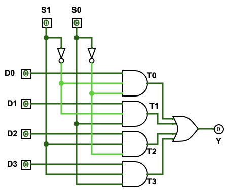
Figure 2.2: Gate-level 4-to-1 multiplexer circuit.
Selection-path wiring reference:
| Path | Data input | Select condition | Meaning |
|---|---|---|---|
| T0 | D0 | select D0 when S1S0 = 00 | |
| T1 | D1 | select D1 when S1S0 = 01 | |
| T2 | D2 | select D2 when S1S0 = 10 | |
| T3 | D3 | select D3 when S1S0 = 11 |
Table 2.3: AND-gate inputs for each selection path in a gate-level 4-to-1 MUX.
- Verify by truth table
- Fix inputs (example): D0=0, D1=1, D2=0, D3=1.
- Set (S1,S0) to 00, 01, 10, 11 and confirm Y matches D0, D1, D2, D3.
- Change D0…D3 and repeat.
Task 2: Build a 2-to-4 decoder using gates
Section titled “Task 2: Build a 2-to-4 decoder using gates”- Place inputs/outputs
- Place input pins A0 and A1.
- Place output pins Y0, Y1, Y2, Y3 (set them as outputs).
- Generate inverted inputs
- Use two NOT gates to generate and .
- Build the four output paths
- Place four AND gates.
- Wire each AND gate according to the table below.
- Connect outputs
- Connect each AND output to Y0…Y3.
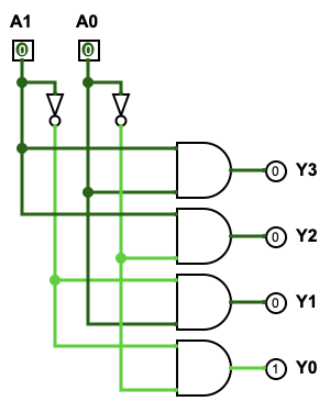
Figure 2.3: Gate-level 2-to-4 decoder circuit.
Output-path wiring reference:
| Output | AND inputs | Input combination | Meaning |
|---|---|---|---|
| Y0 | A1A0 = 00 | assert Y0 | |
| Y1 | A1A0 = 01 | assert Y1 | |
| Y2 | A1A0 = 10 | assert Y2 | |
| Y3 | A1A0 = 11 | assert Y3 |
Table 2.4: AND-gate inputs for each output line in a gate-level 2-to-4 decoder.
- Verify by truth table
- Test inputs 00, 01, 10, 11.
- Confirm exactly one of Y0…Y3 is 1 each time.
Results
Section titled “Results”- 4-to-1 MUX: circuit screenshot + test screenshots proving Y = D0/D1/D2/D3 for S1S0 = 00/01/10/11.
- 2-to-4 decoder: test screenshots proving one-hot outputs.
Extension
Section titled “Extension”Implement a NAND function using only multiplexers:
- Target:
- Constraints: do not build a NAND by chaining an AND + NOT; you may use constant 0/1 sources.
- Hint: for a 2-to-1 MUX, . Try using B as S, and choose D0/D1 based on the NAND truth table.