Datapath Construction
In a single-cycle CPU, the datapath describes how data flows through modules (PC, instruction memory, register file, ALU, data memory, multiplexers) during instruction execution. The datapath is relatively stable; control signals select which routes are active.
In this stage you will not fully automate control yet. You will manually fix or drive control signals and build up the datapath incrementally.
Experiment: Build the datapath for ADDI
Section titled “Experiment: Build the datapath for ADDI”Objectives
Section titled “Objectives”- Understand data flow between PC, instruction decode, ALU, and register file.
- Understand how
ADDIexecutes on the datapath. - Build a minimal working single-cycle datapath that can execute
ADDIwith sequential fetch.
Principles
Section titled “Principles”ADDI(I-type) semantics: (12-bit signed immediate sign-extended to 32 bits).- Single-cycle: fetch/decode/execute/write-back all within one cycle; state updates at the rising edge.
- Minimal assumptions for this stage:
- no branches/jumps/memory
- PC always increments:
- ALU only needs add
Environment
Section titled “Environment”- Simulator: Logisim Evolution
Task 1: PC increment and instruction fetch path
Section titled “Task 1: PC increment and instruction fetch path”- Place a 32-bit register named PC.
- Place a 32-bit adder.
- Place a 32-bit constant 4.
- Place a 32-bit ROM as instruction memory (e.g., address bits = 10).
- Wire PC + 4 back into PC input.
- Because Logisim memories are word-addressed (here 32-bit words), use a splitter to feed PC[11:2] into the ROM address.
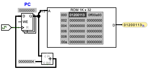
Figure 5.1: PC increment and instruction fetch path.
Verify PC increments by 4 each clock edge and the ROM output changes with PC.
Task 2: Instruction field decode and immediate generation
Section titled “Task 2: Instruction field decode and immediate generation”- Use a splitter to extract:
rd = inst[11:7]rs1 = inst[19:15]imm12 = inst[31:20]
- Use a bit extender to sign-extend 12 → 32 bits to form
imm32.
Task 3: Import ALU and register file
Section titled “Task 3: Import ALU and register file”- Reuse your ALU from the earlier ALU lab as a subcircuit (or recreate it).
- Change datapath widths to 32 bits.
- Import/place the provided
reg_file.circand place ALU + RegFile in the main circuit.
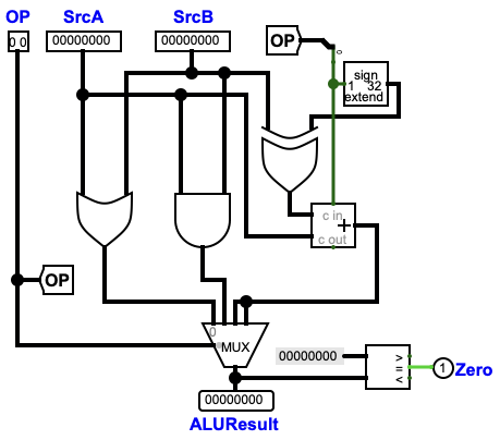
Figure 5.2: Example 32-bit ALU circuit.
Task 4: Wire the ADDI datapath
Section titled “Task 4: Wire the ADDI datapath”- Connect
rs1to RegFileRA1, and RegFileRD1to ALU SrcA. - Connect the sign-extended immediate to ALU SrcB.
- Provide an input pin
ALUControlto select add. - Connect ALU result to RegFile write data
WD. - Connect
rdto RegFile write addressWA. - Provide an input pin
RegWriteto drive the RegFile write enable.
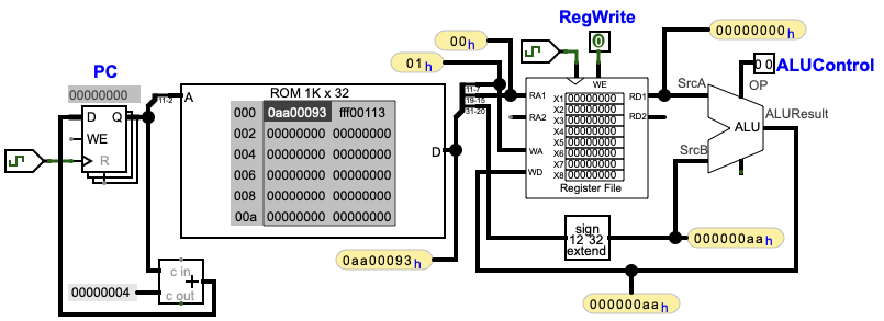
Figure 5.3: Datapath for the ADDI instruction.
Task 5: Verification
Section titled “Task 5: Verification”Design your own verification (refer to the report requirements and questions).
Results
Section titled “Results”- Screenshot of your complete
ADDIdatapath. - At least two
ADDIinstruction test traces: initial register values, instruction, and finalrdvalue. - Explain the roles of PC+4, sign-extension, and ALU in the result.
Questions
Section titled “Questions”- What should RegFile
WEand ALUOP/ALUControlbe set to forADDI? - What breaks if the instruction is not
ADDI? How should a full design solve this? - Why must PC and register writes be clocked (sequential) rather than purely combinational?
- If
immis negative, which part of the datapath ensures correctness? - If you add
ADDlater, which parts can be reused?
Experiment: Add the datapath for LW
Section titled “Experiment: Add the datapath for LW”Objectives
Section titled “Objectives”- Understand the flow “address calculation → memory read → write-back”.
- Use a MUX to select the write-back source.
Principles
Section titled “Principles”LW: .
Compared with ADDI, the address calculation is the same; the difference is the write-back source (memory vs ALU).
Environment
Section titled “Environment”- Simulator: Logisim Evolution
Task 1: Add data memory (RAM)
Section titled “Task 1: Add data memory (RAM)”- Place a 32-bit RAM (e.g., address bits = 10).
- Feed RAM address from ALU result (use ALU[11:2] as word address).
Task 2: Add a write-back MUX
Section titled “Task 2: Add a write-back MUX”- Place a 32-bit 2-to-1 MUX.
- Input 1: ALU result (for
ADDI) - Input 0: RAM read data (for
LW) - Output to RegFile
WD - Control pin
ResultSrc:- 0: write back memory data (
LW) - 1: write back ALU result (
ADDI)
- 0: write back memory data (
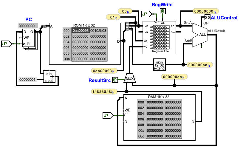
Figure 5.4: Datapath extended to support LW.
Task 3: Verification
Section titled “Task 3: Verification”Design your own verification.
Results
Section titled “Results”- Screenshot of datapath after adding RAM + write-back MUX.
- At least one
LWtest trace: control pins, base register, immediate, memory contents, and finalrd. - Compare the write-back paths of
ADDIvsLW.
Questions
Section titled “Questions”- Why can
LWreuse theADDIALU path? - For one
ADDIand oneLW, what are the correct control-pin settings and operation sequence? - To add
SW, what additional datapath changes are needed?
Experiment: Datapath analysis for R-type, S-type, and B-type instructions
Section titled “Experiment: Datapath analysis for R-type, S-type, and B-type instructions”Complete the provided comparison tables and summaries:
| Comparison item | R-type | I-type |
|---|---|---|
| Uses immediate | ||
Needs rs2 read port | ||
| ALU operand B source | ||
| Accesses data memory | ||
| Write-back source |
Table 5.2: Datapath comparison between R-type and I-type instructions (fill in during the lab).
| Comparison item | R-type | S-type | B-type |
|---|---|---|---|
| Uses immediate | |||
Needs rs2 read port | |||
| Writes register file | |||
| Accesses data memory | |||
| Modifies PC |
Table 5.3: Datapath comparison for R/S/B types (fill in during the lab).