Latches and Flip-Flops
“State” is the internal information a circuit holds at a particular time. In sequential logic, outputs depend on both inputs and stored state. The fundamental storage structure is a bistable circuit with two stable states.
In practice, bistable storage is abstracted into two basic memory elements:
- Latch: level-sensitive
- Flip-flop: edge-triggered
They form the basis of registers, counters, and state machines.

Figure 3.1: D latch symbol.

Figure 3.2: D flip-flop symbol.
A latch is level-sensitive. Its typical behavior is:
- When enable is active (), output follows input: .
- When enable is inactive (), output is latched and holds its previous value.
Some references use to mean enable. This manual uses to emphasize level sensitivity.
Latches are simple and have small delay, but if enable remains active too long, input glitches may propagate to output and cause hazards.
Flip-flop
Section titled “Flip-flop”To avoid the uncertainty of level sensitivity, synchronous digital systems commonly use edge-triggered flip-flops. A flip-flop samples input only at a clock edge (rising or falling), and holds output stable between edges.
For a D flip-flop:
- At the clock edge, updates to the current .
- Between edges, is unaffected by changes on .
This discrete, synchronized state update makes flip-flops the preferred elements for program counters, general-purpose registers, and pipeline registers.
Experiment: Level-triggered vs edge-triggered behavior
Section titled “Experiment: Level-triggered vs edge-triggered behavior”Objectives
Section titled “Objectives”- Understand the essential difference between level-triggering and edge-triggering.
- Observe how a latch and a flip-flop respond to changing inputs.
- Build intuition for clock–state–synchronization.
Principles
Section titled “Principles”A latch is sensitive to the enable level; a flip-flop samples only at clock edges.
Logisim Evolution does not directly provide a D latch, so in this experiment you will build a D latch using basic gates. See Figure 3.3.
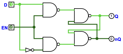
Figure 3.3: Gate-level D latch circuit.
Environment
Section titled “Environment”- Simulator: Logisim Evolution
Task 1: Build a D latch and observe behavior
Section titled “Task 1: Build a D latch and observe behavior”- Inputs/outputs
- Place two input pins: and .
- Place two output pins: and (label it nQ), set them as outputs.
- Generate
- Place a NOT gate and connect to get .
- Build the gated signals and cross-coupled NAND latch
- Place four NAND gates and wire them according to Figure 3.3.
- Verify and observe
- Set , toggle (0→1→0) and check whether follows immediately.
- Set , toggle again and check whether holds the value latched when switched 1→0.
- Tip: if the state becomes abnormal due to wiring order, use Simulate → Reset Simulation.
Task 2: Observe D flip-flop behavior
Section titled “Task 2: Observe D flip-flop behavior”- Inputs/outputs and clock
- Place input pin and output pin .
- Place a Clock component as the clock source.
- Place a D flip-flop and connect clock
- In Memory, place a D flip-flop.
- Connect the clock output to the flip-flop’s CLK pin (triangle-marked).
- Connect data path
- Wire to the flip-flop’s D pin.
- Wire flip-flop Q to output pin .
- Verify and observe
- Toggle multiple times between two clock edges and check whether stays unchanged.
- Trigger one clock edge and check whether updates to the value of at that edge.
- Tip: use a low clock frequency to make edge sampling easier to observe.
Results
Section titled “Results”- Circuit screenshots.
- A table/notes comparing:
- how responds to for a D latch with vs ;
- how updates for a D flip-flop before/after clock edges.
- Write the truth tables for the D latch and D flip-flop and summarize (in your own words) the key difference between level-triggering and edge-triggering. Explain which is more suitable for synchronous register design.
Question
Section titled “Question”- Why do CPUs almost never use level-triggered latches directly as general-purpose register storage elements?
Extension
Section titled “Extension”Read the Logisim Evolution documentation and draw timing diagrams for the D latch and D flip-flop.
Experiment: 4-bit synchronous parallel register
Section titled “Experiment: 4-bit synchronous parallel register”Objectives
Section titled “Objectives”- Understand the structure of a parallel register.
- Understand the role of a synchronous clock.
- Build a multi-bit register using D flip-flops.
- Implement a load-enable (write-enable) control.
- Understand the purpose of asynchronous reset for initialization.
Principles
Section titled “Principles”- Parallel register structure
An -bit register is built from D flip-flops in parallel. All bits share the same clock so the state updates synchronously.
- Load enable
To hold the current value when desired, place a 2-to-1 MUX in front of each flip-flop to select between “keep old value” (feedback) and “load new value”.
- Asynchronous reset
Asynchronous reset clears the register to zero without relying on the clock.
Environment
Section titled “Environment”- Simulator: Logisim Evolution
Task 1: Basic parallel register
Section titled “Task 1: Basic parallel register”- Place four D flip-flops (name them bit0…bit3).
- Add one clock and connect it to all four flip-flops.
- Place four input pins: and connect them to the corresponding D inputs.
- Place four output pins: and connect them to the corresponding Q outputs.
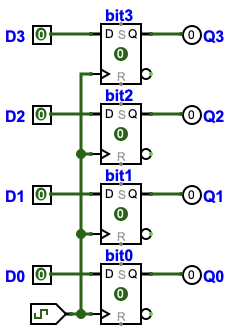
Figure 3.4: Basic 4-bit parallel register circuit.
- Verify by setting inputs (e.g. 1010), triggering clock edges, and observing outputs update.
Task 2: Register with load enable
Section titled “Task 2: Register with load enable”Add a global control signal and place a 2-to-1 MUX before each flip-flop:
- MUX input 0: feedback from current (hold)
- MUX input 1: external (load)
- MUX select:
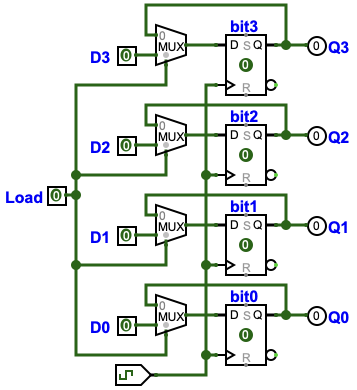
Figure 3.5: 4-bit register with load-enable using MUX feedback.
Verify:
- : outputs update on clock edge.
- : outputs hold their values across clock edges.
Task 3: Asynchronous reset
Section titled “Task 3: Asynchronous reset”Add a global reset signal and connect it to the clear/reset pins of all flip-flops.
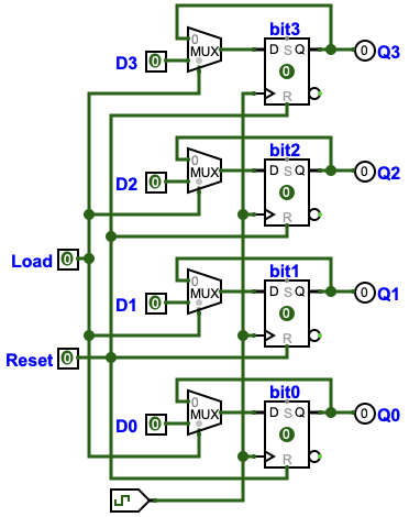
Figure 3.6: 4-bit register with asynchronous reset.
Verify that toggling clears outputs to 0000 immediately, even without a clock edge.
Results
Section titled “Results”- Circuit screenshots.
- Verification screenshots + brief analysis for:
- Write: writes on clock edge.
- Hold: holds across edges.
- Reset: clears immediately.
Questions
Section titled “Questions”- To extend this to an 8-bit register, what changes are required (flip-flop count, MUX count, I/O widths, etc.)?
- When , why is the value “locked” in the register? Explain using the MUX feedback path.
- Where does the “asynchronous” nature of async reset show up? How would you implement a synchronous reset?