Register File
A register file is a set of registers organized as an addressed array.
In CPUs, register files typically provide:
- multiple read ports (e.g., read two source operands in the same cycle)
- at least one write port (write back results on a clock edge)
- address selection for choosing which register to read/write
In this section you will build a simplified multi-port register file: 4 registers × 8 bits, with two read ports and one write port, and observe its read/write behavior.
Experiment: 4×8 multi-port register file
Section titled “Experiment: 4×8 multi-port register file”Objectives
Section titled “Objectives”- Understand the structure: register array + write decoding + read selection.
- Understand the difference between ports:
- the write port is clocked (synchronous write)
- the read ports are address-selected (combinational read)
Principles
Section titled “Principles”1) Interface
Section titled “1) Interface”Registers: , each 8 bits.
Write port:
- : write address
- : write data
- : write enable
- : clock
Two read ports:
2) Behavior
Section titled “2) Behavior”- Synchronous write: when , on the rising clock edge write into .
- Combinational read: , .
3) Implementation idea
Section titled “3) Implementation idea”- Register array: 4 parallel 8-bit registers ()
- Write selection: decode with a 2-to-4 decoder; AND with to form each register’s load/WE
- Read selection: two 4-to-1 MUXes, one for , one for
Environment
Section titled “Environment”- Simulator: Logisim Evolution
Task 1: Build the 4×8 register array and write port
Section titled “Task 1: Build the 4×8 register array and write port”- Place pins: , , , .
- Place 4 Register components (name them ).
- Set bit widths: is 2 bits; and each register are 8 bits.
- Wire to all register inputs; wire to all register clock inputs.
- Decode write address:
- place a 2-to-4 decoder for
- AND each decoder output with and feed to the corresponding register’s enable/write input
Task 2: Build two read ports
Section titled “Task 2: Build two read ports”- Place pins: , , , .
- Set bit widths: and are 2 bits; and are 8-bit outputs.
- Place two 4-to-1 MUXes (select bits = 2).
- Connect outputs to the data inputs of both MUXes.
- Wire to MUX1 select and MUX1 output to .
- Wire to MUX2 select and MUX2 output to .
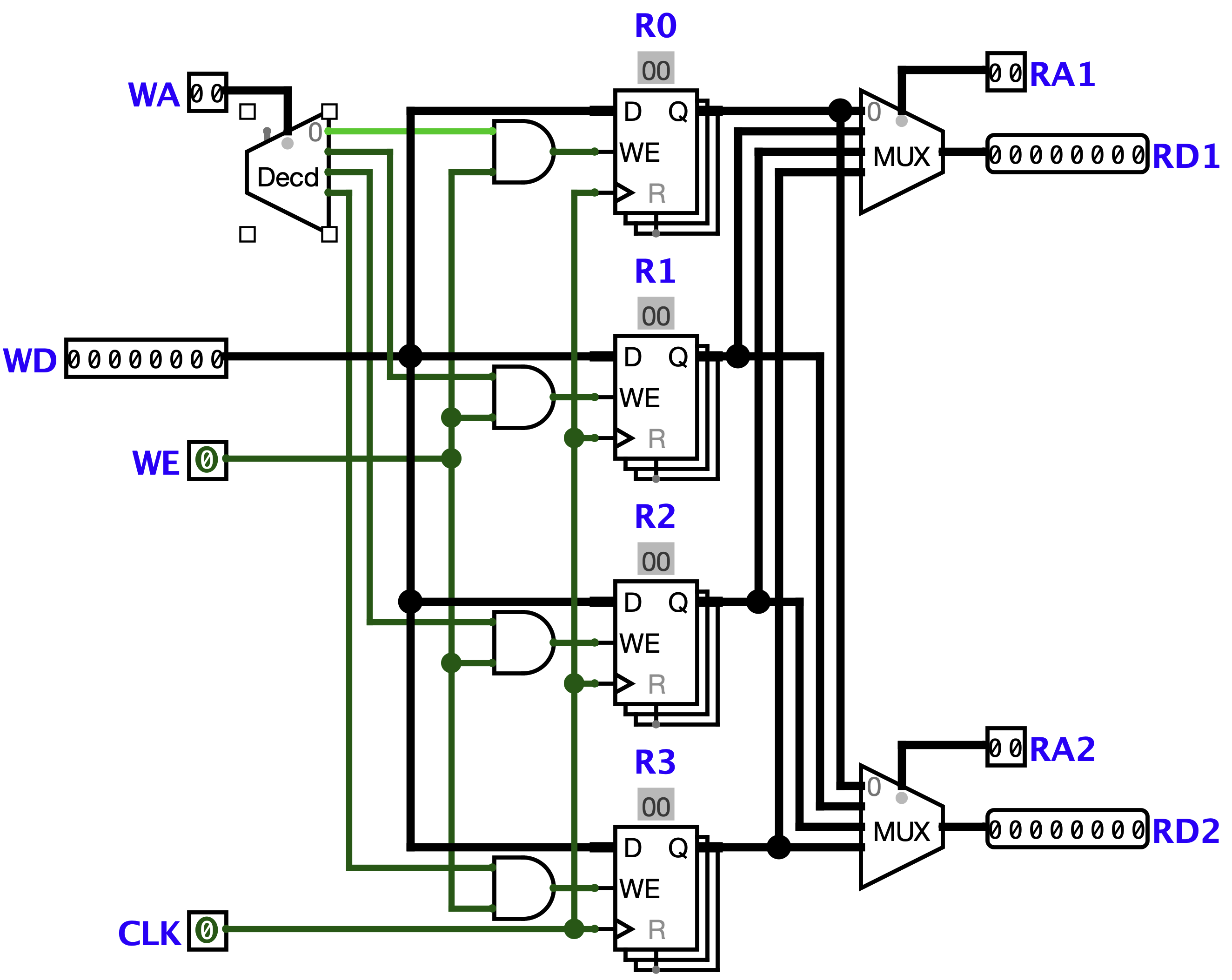
Figure 3.7: 4×8 multi-port register file circuit.
Task 3: Verification
Section titled “Task 3: Verification”Use probes to observe and .
-
Case 1: Write and hold
- Set (write ), , .
- Trigger one rising edge on , then set .
- Change to 0xFF and trigger multiple clocks: should remain 0xA5.
- Set , and confirm both reads output 0xA5.
-
Case 2: Two read ports in parallel
- Write 0x3C to and 0xF0 to (each write requires and a clock edge).
- Set , and confirm , .
- Without clocking, change (e.g. to 00) and observe changes immediately.
-
Case 3: Read/write overlap
- Keep to continuously read .
- Write 0x55 to (set , , , trigger clock edge).
- Confirm reading remains unchanged; then set and confirm .
Results
Section titled “Results”- Circuit screenshot (including any extra probes/displays used).
- Verification notes:
- why writing requires a clock edge
- why changing changes immediately
- why values do not change when even if the clock toggles
Questions
Section titled “Questions”- If you extend from 4 registers to 8, which key structures must change?
- If and a write happens in the same cycle, do you observe as the old value or new value? Explain based on your structure (read is combinational; write happens at the edge).
Extension
Section titled “Extension”- Make hard-wired to 0 (always reads 0 regardless of writes).
- Add a global Reset to clear all registers.
- Scale up to .